BCD 0o27 - Hardware Assembly Guide
The assembly guide for the 2023 badge BCD-0o27 of the BalCCon2k23 conference.
Version: 0x00
Applies to: HW Rev. 0x06
This guide describes how to manufacture the BalCCon Cyberdeck 0o27 (BCD-0o27). The BCD-0o27 was the conference badge for BalCCon 2k23. It serves as a development platform and will likely be used in future conferences as well. To learn more about the BCD-0o27 check out the BalCCon Cyberdeck 0o27, aka BCD-0o27 Hackaday article or future posts on this site.
General remarks
Manufacturing a small number of badges can be rather expensive. It might be cheaper to purchase a badge at one of the future BalCCon conferences or team up with others to produce higher numbers. Purchasing from the conference will have the added effect, that you support a community driven conference that is not making any profit and completely independent of any commercial sponsors or interest.
This assembly guide is applicable to the source files provided with it and does not necessarily apply to any past or future version of the badge. See "applies to" just after title.
The focus of this guide is on the hardware and software aspects will only be covered when relevant for testing.
Download the required zip file to get started:
Parts sourcing
In order to save delivery and customs cost, as little as possible different vendors where chosen. Of course, parts can also be sourced in different places as most of the parts are quite standard. The following sources were used for parts in the past:
| Part | Source | Reference Price | Remarks |
|---|---|---|---|
| Display (1.8 "1,8 inch 128x160 SPI) | EC-Buying Ali Store | 2$ | The welded type is needed - make double sure you get the right one that fits the footprint! Also, different configurations of the driver chip for this lcd exist. If its not the right variant, the display driver needs to be adapted. Usually the variant is indicated by the tab of the screen protector foil, but unfortunately the marking is inconsistent. So switching the source without verifying is not recommended. |
| 3M 9448A Double-Sided Transparent Adhesive Tape | Amazon | 7.5$ | 2mm transparent double sided repair tape, usually used for pinning down lcds on mobile phones. |
| 1x18650 battery holder | Yikeshu Store | 0.5$ | The holder has a small knob on the bottom that needs to be cut away. Otherwise the holder will not sit flush on the board. |
| Jumper 2.4mm | IBUW Official Store | 0.23$ / 100pcs | Nothing fancy, just jumpers ;-) |
| PCB | jlcpcb | variable | There is a fix engineering fee of about 30$ and depending on the amount of boards ordered other fees apply. 200 boards will cost around 200$ |
| Other parts | LCSC | variable | All other parts are sourced at lcsc. lcsc parts can also be ordered through jlcpcb if ordering assembled boards. |
Manufacturing
The prototypes have been manufactured at JLCPCB. For the first prototype only the board was ordered and it was assembled by hand. Following prototypes where ordered with and assembled by JLCPCB, except the display and the battery holder.
Of course, other manufacturers can be chosen. But then at least another prototype run should be made for the manufacturing of the board. Assembly by a different entity does not require a new prototype run.
Board Manufacturing
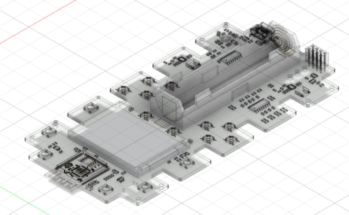
The PCB is a impedance controlled four layer board with the following specifications:
| Parameter | Value |
|---|---|
| Material | FR4 |
| Layers | 4 |
| Stackup | signal - ground - power - signal |
| Outer copper weight | 1oz |
| Inner copper weight | 0.5oz |
| Impedance control | Yes - Specifics see below |
Impedance Control
The PCB should be impedance controlled to ensure the USB / serial lines have proper 90 ohm. The board stack should look like this:
Known Inconveniences
Even though initially trace width for the USB / serial line has been chosen as 0.286mm (11.26 mil), this was by accident reset to 0.2mm in the development process. Therefore impedance is not exactly matched. However, the prototypes work and we leave it at that to avoid having to spend the money on yet another prototype.
Further, the footprint for the battery holder does not have a drilled hole to fit the knob on the bottom of the battery holder used for alignment. To avoid adapting the footprint and ordering another prototype we simply cut the knob with an box cutter from the battery holder before assembly.
Last but not least, some of the parts around the display are very close to it. This is not a problem for the current badge, but when 3d printing a case that has a display frame, those parts can get in the way and need to be omitted in the frame.
The artwork has been placed on the board after the last prototype was ordered. The decision was made not to order another prototype as the art "should be fine". Lets see ;-).
Ordering the Board at JLCPCB
To order the board from jlcpcb go to jlcpcb.com. Upload the gerber.zip file to jlcpcb by choosing "Add gerber file" from the "Get instant quote" bar:
Choose the following settings:
- Base Material: FR-4*
- Layers: 4*
- Dimensions: 149.85 * 74.22* (will be corrected by jlcpcb to 149.9 mm* 84.2 mm automatically)
- PCB Qty: However many you want
- Product Type: Industrial/Consumer electronics*
- Different Design: 1*
- Delivery Format: Single PCB*
- PCB Thickness: 1.6*
- PCB Color: Purple
- Silkscreen: White*
- Material Type: FR4-Standard TG 135-140*
- Surface Finish: HASL (with lead)*
- Outer Copper Weight: 1oz*
- Inner Copper Weight: 0.5oz*
- Specific Layer Sequence: yes
- L1(Top Layer): BCD-Oo26-F_Cu.gbr
- L2(Inner Layer 1): BCD-Oo26-In1_Cu.gbr
- L3(Inner layer2): BCD-Oo26-In2_Cu.gbr
- L4(Bottom layer): BCD-Oo26-B_Cu.gbr
- Impedance Control: yes
- JLC04161H-7628
- Via Covering: Tented*
- Min via hole size/diameter: 0.3mm(0.4/0.45mm)*
- Board Outline Tolerance: +-0.2mm(Regular)*
- Confirm Production File: yes
- Remove Order Number: yes
- Flying Probe Test: Fully test*
- Gold Fingers: No*
- Castellated Holes: No*
- Advanced Options: Use defaults
- 4-Wire Kelvin Test: No*
- Paper between PCBs: No*
- Appearance Quality: IPC Class 2 Standard*
- Silkscreen Technology: Ink-jet/Screen Printing Silkscreen*
- Package Box: With JLCPCB logo
* = should be preselected by default. Double check if your gerber was properly read.
If you want to order also assembly, then jump to [[BCD 0o26 - Hardware Assembly Guide#Assembly with JLCPCB]]. Otherwise choose your build time and save the order to cart. Then go through the checkout process.
Once your order has been processed, you will receive an email to check the processed gerbers (if you do not receive an email within a day or two check in your account on the webpage). You should now check the gerbers that everything is correct. Pay special attention that the order number is really removed, as sometimes the removal of the order number is forgotten! You would see the order number either at the front or back silkscreen (if its on the rails - which may be automatically added by jlcpcb for manufacturing its ok, as you will break the rails away anyways).
Assembly
For assembly, you should solder all parts except the display and the battery holder first. Then it is recommended to solder the display and only after that the battery holder, as access with the soldering iron will be easier.
Assembling the Display
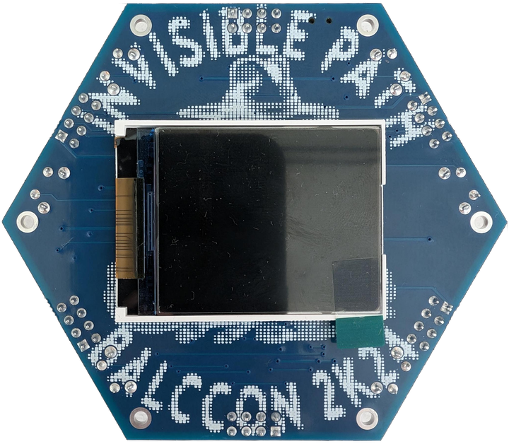
Display will be soldered directly to the board and then tucked down with 3M 9448A extremely strong double-sided transparent adhesive tape.
It is crucial to get a good solder connection, as the display will not function properly otherwise. It also should be noted, that even if the solder connections look good under the microscope, sometime the connection between the board and the flex pcb part of the display are not good enough. Therefore I recommend to use the following technique:
- Add solder to all the fingers of the footprint on the pcb.
- Position the flex pcb of the lcd correctly and then use the hot soldering iron on at least 4 fingers where the whole in the contact is to melt the solder below. This will hold the connector nicely in place.
- Now, for each finger of the connection heat it properly with the soldering iron and add solder. Make sure to melt also the solder beneath the connector. Make sure that the connection is solid. It is likely necessary that you push the flex pcb down to ensure a good connection without gap.
Once the display is soldered, I recommend soldering the rest of the components and test the display before taping it down. Make sure you do not flap around the display unnecessarily as this might result in brocken contacts or solder connections.
Once everything works fine, use the double-sided adhesive tape to fix the display in place. I recommend adding on strap of tape top to bottom on the left side between the flex pcb and the display and the pcb of the badge and adding horizontal stripes of tap to the large, free surface below the display. Then place a towel on the display and add weight (eg. books) to weigh it down for 24 hours to ensure good adhesive connection.
Soldering the Battery Holder
Soldering the battery holder is straight forward. Just make sure you cut away the know on the bottom of the holder, as the PCB does not have a hole and forgetting to do so will result in the holder not sitting flush and potentially having a poor solder connection. Also make sure the + and - markings on the holder match the markings on the PCB.
Soldering the USB-C connector
When soldering the USB-C connector make sure that no residual flux or cleaning agent gets in the connector and shorts it out. Otherwise soldering is straight forward.
Soldering the ESP32-S3
Ensure that you also solder the ground connections on the bottom. The datasheet specifies that the ESP32-S3 will still work without having those connections properly soldered, but better safe than sorry.
Soldering the other parts
Soldering of all other parts is straight forward and beyond what is usual does not require any special attention. Pin 1 is marked by a white dot on the PCB. If unsure double check with the pcb layout.
Assembly with JLCPCB
Assembly is straight forward. After uploading your gerbers and setting all the necessary parameters for the PCB as described in [[#Ordering the Board at JLCPCB]]select "PCB Assembly":
Choose the following parameters:
- PCBA Type: Standard (Needed for color choice and some of the parts)
- Assembly Side: Top Side
- PCBA Qty: Choose how many of the boards you want assembled
- Edge Rails/Fiducials: Added by JLCPCB
- Confirm Parts Placement: Yes
Then agree to the terms and conditions and push "Confirm". On the side that is now displayed, select next to be able to add the BOM file and the CPL file. The BOM file is found in the folder "production" and is named "bom.csv". The CPL file is also in the folder "production" and named "positions.csv". Add the two files and choose "Process BOM & CPL".
You will now see a list of all the parts. If all parts are in stock and everything is well you should see a warning that 3 parts are not selected. Verify that those parts are:
- The LCD Display (LCD1)
- The TAG Connect footprint (J3)
- The battery holder (BT1)
If other parts are not selected this may be due to part shortage. You have two options. Either search for a alternative part with the parts browser (recommended) or place an order and source the rest of the parts somewhere else and hand assemble. In any case, it might be valuable to contact JLCPCB to ask if they expect stock to go up soon and if they may reserve all parts needed for your order. They might do this for large orders.
Now choose next and choose "Do not place" in the warning dialog that states that "The project has unselected parts.". On the next screen click next as well and ignore wrongly placed parts. You will be able to confirm parts placement after the order is complete and they verify it in the factory. Save the order to the card and proceed with payment.
You will receive an email after the order has been processed by the factory. Make sure to verify the PCB as described in [[#Ordering the Board at JLCPCB]]. Also verify the parts placement. Once all of this is done log into your account and confirm the production files for the PCB and assembly.
Testing
To test the badge download the firmware from the git repository and run it. This should allow to test if the display, the LEDs and the buttons are working fine. A test firmware might be developed in the near future.
Comments ()